
The Quest for Room-Temperature Emission in GeSn
GeSn alloys are a promising material for integrating infrared light sources directly on silicon chips. In his PhD project at the Department of Physics and Astronomy, Martin Aagaard explored how electrons move and recombine in this material. He worked on uncovering why making GeSn emit light efficiently at room temperature is still a challenge, and what it will take to overcome it.

From Silicon Platforms to Lasers: Why GeSn Matters
Silicon has long been the foundation of modern information technology, but it is not good at emitting light. This has slowed the development of fully integrated photonic chips that can combine computation and communication on the same platform. That is where germanium-tin (GeSn) comes in.
GeSn is a semiconductor alloy that can be grown on silicon and tuned to behave more like a direct bandgap material. This means it can emit light more efficiently, potentially enabling Group IV-based lasers and detectors for use in telecommunications, sensing, and quantum technologies.
But getting GeSn to perform well at room temperature remains a major hurdle. That is the challenge Martin Aagaard set out to address in his PhD research, combining advanced spectroscopy, modeling, and materials analysis.
Key Findings
- Carrier lifetimes in GeSn remain long even at higher temperatures (meaning light-emitting states are still populated for some time), but light emission drops due to population shifts from the Γ- to L-valley
- A k·p-based model confirmed that most electrons at room temperature reside in the non-radiative "dark" L-valley, limiting light output
- Upconversion detection and ultrafast spectroscopy allowed access to the photoluminescence of GeSn across a broad spectral and temporal range
- Achieving strong room-temperature emission requires increasing the Γ-L energy separation, for example through strain or tin content
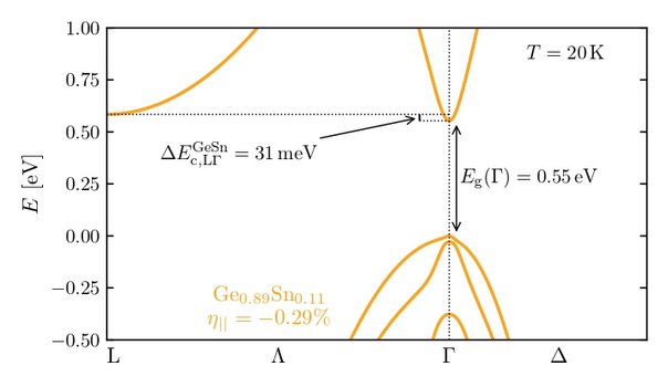
The Valley Problem: Where the Electrons Go
A central difficulty in GeSn is that electrons excited by light do not always emit light in return. Instead, many of them relax into a non-radiative state called the L-valley, where they lose their energy as heat rather than photons.
This competition between the light-emitting Γ-valley and the “dark” L-valley is a fundamental problem when designing GeSn light sources for room-temperature operation.
To understand this issue, Martin used time-resolved photoluminescence spectroscopy (TRPLS), a method where the material is excited with short laser pulses and the decay of its emitted light is measured over time. This allowed him to study how long electrons stayed in the emitting states under different conditions, and how their distribution changed with temperature and laser intensity.
The experiments showed that GeSn emits strongly at low temperatures, with sharp peaks in the mid-infrared range. But as the temperature rises, the total light output drops sharply while the carrier lifetime remains largely unchanged.
This was surprising. Typically, when luminescence drops, carrier lifetimes shorten. But Martin’s results suggested that something else was happening: electrons were still present, but they were no longer in a state that could emit light efficiently.
Using a theoretical model based on k·p theory, he was able to show that at room temperature, up to 88 % of carriers populate the non-radiative L-valley. This explained the emission drop-off and confirmed that the key to improving performance lies in shifting the energy balance to favor the direct Γ-valley.
How to Make GeSn Emit Light at Room Temperature
Martin’s results point to a clear conclusion: to achieve strong mid-infrared light emission at room temperature, the energy difference between the Γ-valley and the L-valley must be increased. In other words, the Γ-valley must be made even more favorable for electrons, so that they stay there long enough to emit photons.
According to his modeling and measurements, this could be done by:
- Increasing the tin content in the alloy, which narrows the bandgap and can favor the direct Γ-valley
- Applying tensile strain
- Optimizing material quality to reduce non-radiative recombination paths
Martin’s work helps us to understand how it is possible to overcome the room-temperature bottleneck. It also confirms that the challenge is not simply material defects but intrinsic band structure competition.
How Did They Do It?
To investigate how GeSn emits light and how carriers behave inside it, Martin Aagaard used a combination of time-resolved optical techniques and theoretical modeling:
- Upconversion Detection Module: A custom-built setup that enabled detection of mid-infrared emission using standard silicon detectors. This made it possible to study GeSn photoluminescence over a broad spectral range with high sensitivity.
- Time-Resolved Photoluminescence Spectroscopy (TRPLS): Used to measure how long electrons remain in light-emitting states after laser excitation.
- Transient Reflectivity (TR): A complementary method that measures changes in reflectivity caused by changes to the material following laser excitation.
- k·p Band Structure Modeling: This theoretical approach allows to simulate how electrons occupy different valleys (Γ and L) in the GeSn band structure under varying conditions, explaining observed trends in his experiments
Combining these methods helped further the understanding of electron dynamics in the material. This allowed among others to find the luminescence lifetime of GeSn, but also identified the of contributions due to strain waves following laser excitation.
Why Does It Matter?
The success of GeSn-based light sources could bring us closer to fully integrated silicon photonics by combining data transmission, sensing, and computation on a single chip. Martin’s research uses experimental methods that directly probe the optical properties of GeSn, and help identify the current bottlenecks, to achieve CMOS compatible GeSn lasers operating at room temperature.
By combining theory, experiment, and technical innovation, his work contributes valuable insight into carrier dynamics and material behavior under realistic device conditions. It also opens new pathways for developing mid-infrared light sources that are both compact and CMOS-compatible.
If you are working on related materials or applications, we invite you to reach out to our Center Manager to discuss potential collaborations or shared research opportunities.
More information in the following publications:
[1] Luminescence properties of GeSn laser materials: influence of buffered-substrates
M. Aagaard, O. Concepci´on, D. Buca, Z. Ikonic, and B. Julsgaard
[2] Measurement and modeling of strain waves in germanium induced by ultrafast laser pulses
M. Aagaard and B. Julsgaard
[3] Tunable infrared upconversion module for the 1.9 to 5.5 μm range
P. Tidemand-Lichtenberg, M. Aagaard, A. S. Ashik, C. Pedersen, and B. Julsgaard
[4] Two- and three-photon absorption in silicon for above-bandgap photon energies
M. Aagaard, S. P. S. Jessen, R. M. Turtos, P. Balling, and B. Julsgaard